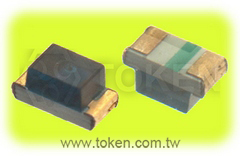
SMD Infrared Receiving Light Sensor (PT-B1-DC-0603-940) Chip
DeMint SMD IR phototransistors achieve the second generation of optical axis keyboard.
Optical axis keyboard is a new generation keyboard which join the new optical sensor recognition technology in recent years. By replacing the traditional metal contacts for the optical sensor components, use optical media as a bridge. Because there is no contact, so it will not wear.
Optical axis technology takes advantage of infrared optical induction. There is no abrasion during conduction due to no contact point. The waveform of Optical signal pulse output is clean and noise-free. The keyboard response speed only takes 1ms. Thanks to the new optical sensors - SMD IR phototransistors (PT-B1-DC-0603-940) is the most critical component in optical axis applications.
The (PT-B1-DC-0603-940) surface mounted infrared receiving light sensor features fast response speed, stable performance, low current loss in static, and anti-strong light interference. The effective control distance is greater than 1.5 meters.
For the convenience of installation in all kinds of products in any position, different sizes are available upon request. So that product consistency is better, more market competitiveness. It is also achievable to provide the bright current / dark current (bright resistance / dark resistance) for the most suitable product.
Download complete specification SMD Infrared Receiving Light Sensor (PT-B1-DC-0603-940) PDF.
- Replace the traditional CDS photoresistor. No Cadmium and lead free with RoHS compliant.
- Suitable for all kinds of light control lighting products, such as security monitoring machine, small night lights, lawn lights, solar lights and so on.
- Auto-adjust background light, such as LCD, mobile phone, camera, digital photo frame, GPS navigation.
- Control all kinds of optical control video products and all kinds of optical control testing equipment.
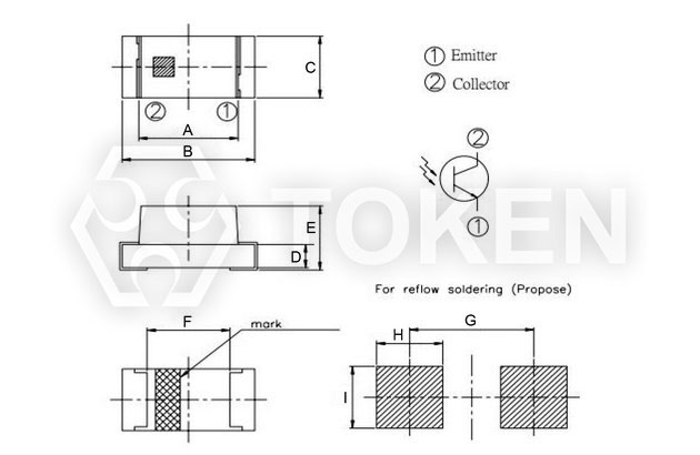
| Dimensions & Configurations Chip (PT-B1-DC-0603-940) Unit: mm | ||||||||||
|
||||||||||
| Part NO. | A (mm) | B (mm) | C (mm) | D (mm) | E (mm) | F (mm) | G (mm) | H (mm) | I (mm) | |
| PT-B1-DC-0603-940 | 1.2 ± 0.2 | 1.6 ± 0.2 | 0.8 ± 0.2 | 0.3 ± 0.2 | 0.8 ± 0.2 | 1.0 ± 0.2 | 1.5 ± 0.2 | 0.8 ± 0.2 | 0.8 ± 0.2 | |
| Electro-Optical Characteristics (Ta=25°C) PT-B1-DC-0603-940 | ||||||
| Parameter | Symbol | Condition | Min. | Typ. | Max. | Unit |
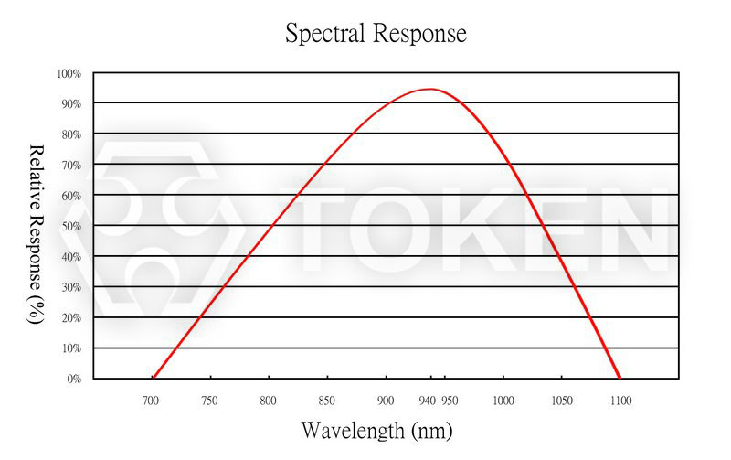
| Peak Wavelength | λp | \ | - | 940 | - | nm |
| Spectral Response Bandwidth | λ | \ | 700 | - | 1100 | nm |
| Operating Voltage | Vcc | \ | - | 5 | - | V |
| Collector-Emitter Breakdown Voltage | Bvceo | Ice=100µA Ee=0mW/cm2 |
30 | - | - | V |
| Emitter-Base Breakdown Voltage | Bvceo | Ice=100µA Ee=0mW/cm2 |
3 | - | - | V |
| Collector-Emitter Saturation Voltage | IL(3) | Vcc=5V Ev=0Lux |
- | - | 0.4 | V |
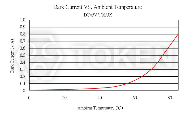
| Collector Dark Current | Id | Vcc=5V Ev=0Lux |
- | - | 0.1 | μA |
| IR Receiving Current | IL(4) | Vcc=5V/940nm IR LED Ee=1mW/cm2 |
- | - | 0.1 | μA |
| Rise Time | tr | Vcc=5V Ev=30Lux RL=1000Ω |
4.5 | μs | ||
| Fall Time | tf | 4.5 | ||||
| Electro-Optical Characteristics (Ta=25°C) PT-B1-DC-0603-940 | ||||
| Parameter | Symbol | Rating Value | Unit | |
| Operating Voltage | Vcc | Min. | Max. | V |
| 1 | 10 | V | ||
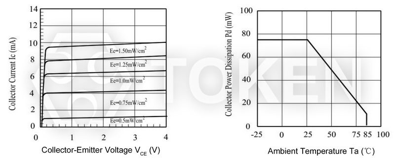
| Power Dissipation | Pc | 75 | mW | |
| Operating Temperature Range | Topr | -25 ~ +85 | °C | |
| Storage Temperature | Tstg | -40 ~ +100 | °C | |
| Relative Spectral Sensitivity vs. Wavelength (PT-B1-DC-0603-940) | |
|
| Dark Current vs. Ambient Temperature (PT-B1-DC-0603-940) | |
|
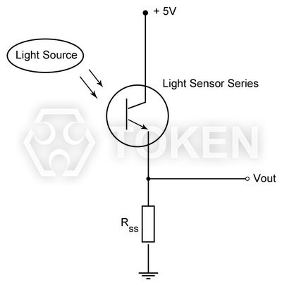
| Photo Current Measurement Method (PT-B1-DC-0603-940) | |
|
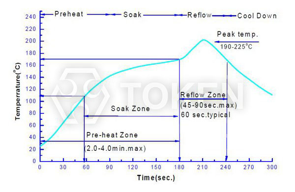
| Recommended Reflow Chart (PT-B1-DC-0603-940) | ||
|
||
| Characteristic of Temperature Curve | Reference Settings | |
| Average Heating Speed (Tsmax to Tp) | Max. 3°C / Sec | |
| Preheating: Minimum Temperature | (Tsmin) | |
| Preheating: Maximum Temperature (Tsmax) | 150°C | |
| Preheating: Time (tsmin to tsmax) | 60 ~ 120 Sec | |
| Reflow Temperature: Temperature (TL) | 183°C | |
| Period of Reflow: Time (TL) | 60 ~ 150 Sec | |
| Peaking Temperature (TP) | 225°C | |
| Within the Actual Peak Temperature (tp) 5°C | 10 ~ 30 Sec | |
| Cooling speed | Max. 6°C / Sec | |
| 25°C Time required to rise to peak temperature | Max. 6 minutes | |
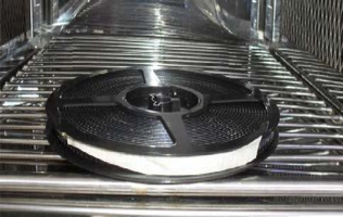
- Without opening the original wrapper, the recommended storage environment is: 5°C ~ 30°C, Humidity less 85%.
- After opening the original wrapper, the recommended storage environment is: 5°C ~ 30°C, Humidity less 60%.
- This product is humidity sensitive device. In order to avoid moisture absorption after unpackage, it is recommended that the opened packaging be stored in an airtight container with desiccant.
- After opening the package, the original should be used within 12 hours.
- If the desiccant fails or the device is exposed to air for more than 12 hours. Should be used for dehumidification treatment at 60°C / 24H.
- Use instructions before soldering this product. After opening the original wrapper, product exposure and humid environment. Product may be damaged during soldering.
- Description of the storage: Products with exposure time exceeding the specified time must be baked according to the baking conditions listed below. The following downgrade table determines the maximum amount of time that this product can be exposed to the humidity and temperature conditions listed. (Unit: Day)
- Baking conditions: No need to bake all the products. Baking is required only if the following criteria are met:
- A: Products that have been removed from the original package;
- B: Exposure to humid environments over time which list in Relative Humidity Table.;
- C: Products that have not been soldered. Reflow soldering of parts within one hours after baking, or immediately store the part in a container of relative humidity less than 20%. The product should be baked in its original reel under 60°C for 24 hours. The exposure time of the products after this baking process is again determined by the moisture sensitivity table above.
| Temperature | Maximum Relative Humidity (%) | ||||||
| 30% | 40% | 50% | 60% | 70% | 80% | 90% | |
| 30°C | 9 | 5 | 4 | 3 | 1 | 1 | 1 |
| 25°C | 12 | 7 | 5 | 4 | 2 | 1 | 1 |
| 20°C | 17 | 9 | 7 | 6 | 2 | 2 | 1 |
|
|
||||||||||||||||||||
- It can be used for up to 100,000 hours at rated current and rated voltage.
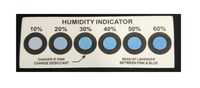
- The card with "Humiditor" in the bag is the humidity monitor card.
- If there is no humidity in the bag, then the color in the black circle of the monitor card is blue as shown in Figure (1).
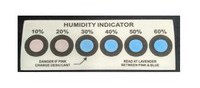
- If humidity card "20%" corresponds to the black circle showing the color is pink, then bake and dehumidification the product as shown in Figure (2).
- Humidity card indicates packaging bag humidity conditions.
|
|
||||||||||||||||||||
- Electrostatic and surge will cause changes in product characteristics, such as positive voltage dropping, etc.
The situation is serious, even damaging the product. - During the whole process (production, testing, packaging, etc.), who might contact with chip phototransistor,
do measures to prevent and eliminate static electricity. - All relevant equipment and machines should be properly grounded. Grounding AC resistance is less than 1.0 Ω,
the worktable needs to cushion surface resistance 106 Ω ~ 109 Ω Table Mat. - The ion fan must be installed on the environment and equipment that produce electrostatic easily.
- Operation process, operators need to use anti-static bracelet, anti-static cushion, anti-static overalls, work shoes, gloves, anti-static capacitors.
- The resin package of the Chip Light Sensor product is quite fragile. Do not scrape the encapsulated resin part with a hard, sharp object.
Should also be very careful when using tweezers to clamp the SMD Light Sensor. - Do not directly use the hand to take the Chip Light Sensor products.
The direct use of hand to get the chip phototransistor will not only pollute the surface of the chip packaging resin,
but also may be due to static factors such as chip product performance changes. - Do not exert excessive pressure on Chip Light Sensor, especially when Chips are in high temperature (for example, during reflow soldering).
Excessive pressure may directly affect the inner chip and the gold wire. - Chip phototransistor working environment and chip adaptation of the material sulfur elements and compounds can not exceed 100PPM.
- The module material cannot be stacked together and may damage the internal circuitry.
- Not available in PH<7 acidic sites.
|
||||||||||
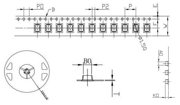
| ITEM | W | A0 | B0 | D | F | E | K0 | P0 | P2 | P | T |
| DIM | 12 | 3.0 | 3.7 | 1.5 | 5.5 | 1.75 | 2.6 | 4.0 | 2.0 | 8.0 | 0.35 |
| TOLE | ±0.3 | ±0.1 | ±0.1 | ±0.1 | ±0.1 | ±0.1 | ±0.1 | ±0.1 | ±0.1 | ±0.1 | ±0.05 |
| Order Codes (PT-B1-DC-0603-940) | ||||||||||||||||||||||||
| PT | - | B1 | - | DC | - | 0603 | - | 940 | ||||||||||||||||
 | | | | | ||||||||||||||||||||
|
|
|
|
|
||||||||||||||||||||